使用宽带电压和电流反馈运算放大器时的应用基础
Keep in mind that applications requiring flexibility in the gain setting network will benefit from the gain bandwidth independence of the current feedback (CFB) design. As described inPart 1, the loop gain equation for a CFB includes only the feedback impedance while the gain element can be varied freely with minimal bandwidth interaction. The following examples exploit that advantage in several situations where a CFB would be the preferred solution.
Example A
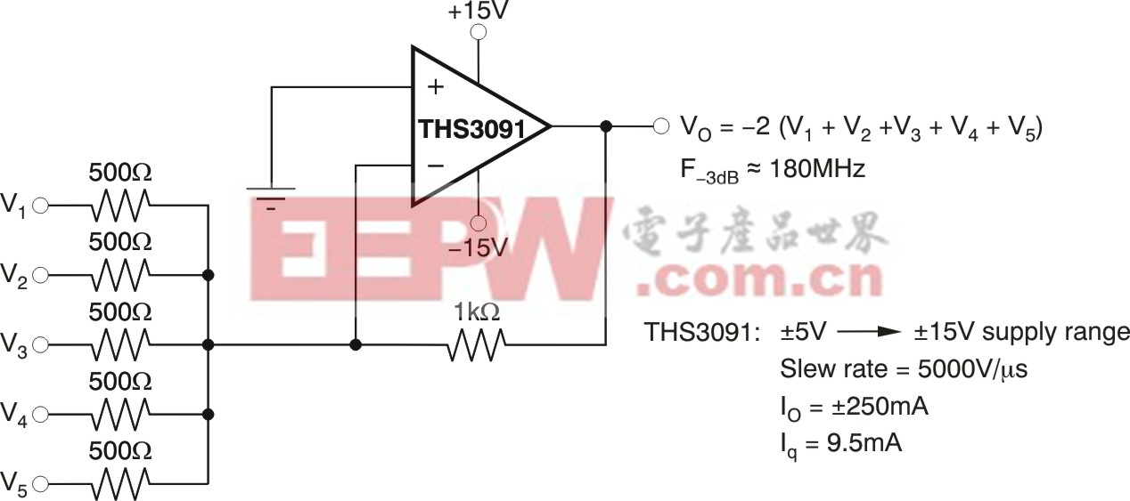
If an inverting summing amplifier is required with a signal bandwidth that is independent of the number of channels summed or the required gains in those channels, a CFB amplifier should be used.Figure 1shows an example of this approach using the high output voltage and current THS3091.
(Click to Enlarge Image)
Figure 1. Inverting summing amplifier using the high voltage/current THS3091.
Here, we assume a 0 Ω source for each of the signal sources where each channel would see a gain of "2 V/V. For these CFB designs, the feedback resistor is first picked to be close to the recommended value for that particular CFB amplifier. Then, each input resistor should be selected according to the gain required by that channel.
Recall that this circuit implemented with a voltage feedback (VFB) has a bandwidth set by the noise gain (NG). For instance, five channels summed with a gain of -2 V/V will have a noise gain of 11. This condition would set a bandwidth for all five channels reduced to the [gain bandwidth product (GBP)]/11 even though each signal only sees a gain of -2 V/V. Using a CFB for this application retains the bandwidth much better because the parallel combination of all gain resistors does not enter strongly into the loop gain equation.
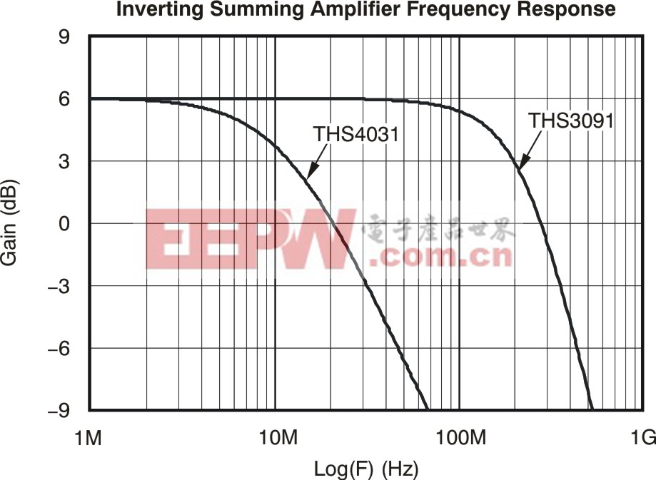
By way of comparison,Figure 2simulates a single channel of Figure 1 using first the CFB TH3091, then a similar VFB THS4031. The THS4031 is a low-noise, high-voltage VFB that offers approximately 200 MHz GBP.
(Click to Enlarge Image)
Figure 2. Comparative frequency response for one channel of Figure 1 using THS3091 and THS4031.
The circuit of Figure 1 produces a noise gain of 11, which shows up as a signal bandwidth close to 18 MHz for the THS4031, while the THS3091 gives about 200 MHz for each channel.

加入微信
获取电子行业最新资讯
搜索微信公众号:EEPW
或用微信扫描左侧二维码