使用宽带电压和电流反馈运算放大器时的应用基础
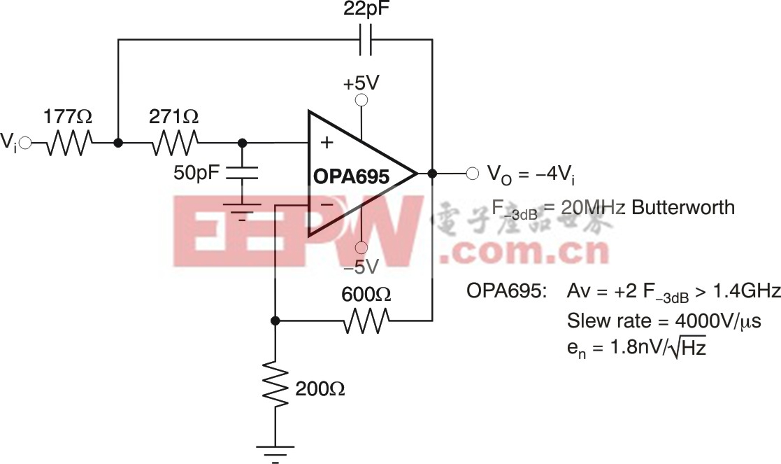
Figure 5shows an example 20 MHz low-pass Butterworth filter implemented using the CFB OPA695 that gives a passband gain of +4 V/V.
(Click to Enlarge Image)
Figure 5. Second-order, low-pass, 20 MHz Butterworth filter using the CFB OPA695.
The resistor values have been adjusted slightly from an ideal analysis to account for the amplifier bandwidth effects and hit the desired frequency response exactly.
In this design, the OPA695 gives an amplifier bandwidth >400 MHz at a gain of +4 V/V (12 dB). This bandwidth gives a 20x margin to the desired filter poles. It is this bandwidth margin that allows the filter poles to be implemented with minimal production variation and holds the stop band rejection down to higher frequencies. All Sallen-Key filters show an increasing gain (or reduced stop band rejection) at very high frequencies as the closed loop output impedance of the amplifier increases sufficiently to support a feed through path through the filter feedback capacitor.
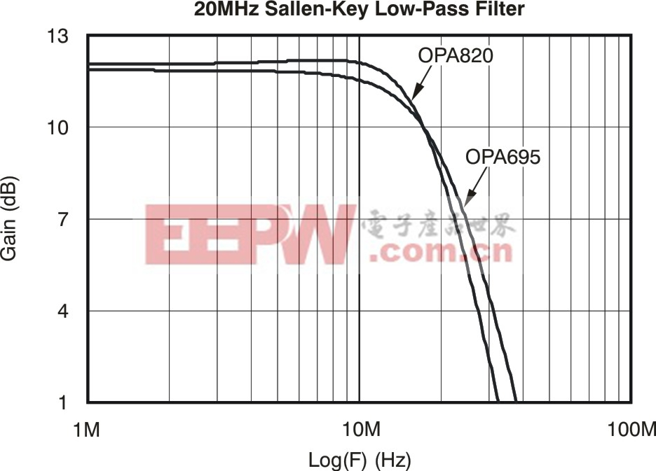
As a comparison,Figure 6shows the filter of Figure 5 simulated first with the OPA695 and then with the VFB OPA820. Operating at a gain of +4 V/V, the OPA820 will have a bandwidth of about 80 MHz.
(Click to Enlarge Image)
Figure 6. Second order, low-pass 20 MHz Butterworth Sallen-Key filter.
The OPA695 implementation hits the desired maximally flat Butterworth design with a 20 MHz cutoff almost exactly. The OPA820 placed into the same circuit shows a slight peaking and reduced bandwidth as predicted. This performance contrasts with the MFB filter discussed in Part 1 of this article, where a VFB is preferred and the effect of finite amplifier gain bandwidth product (GBP) moves the actual poles on a constant 0 circle to lower Q.
Example D
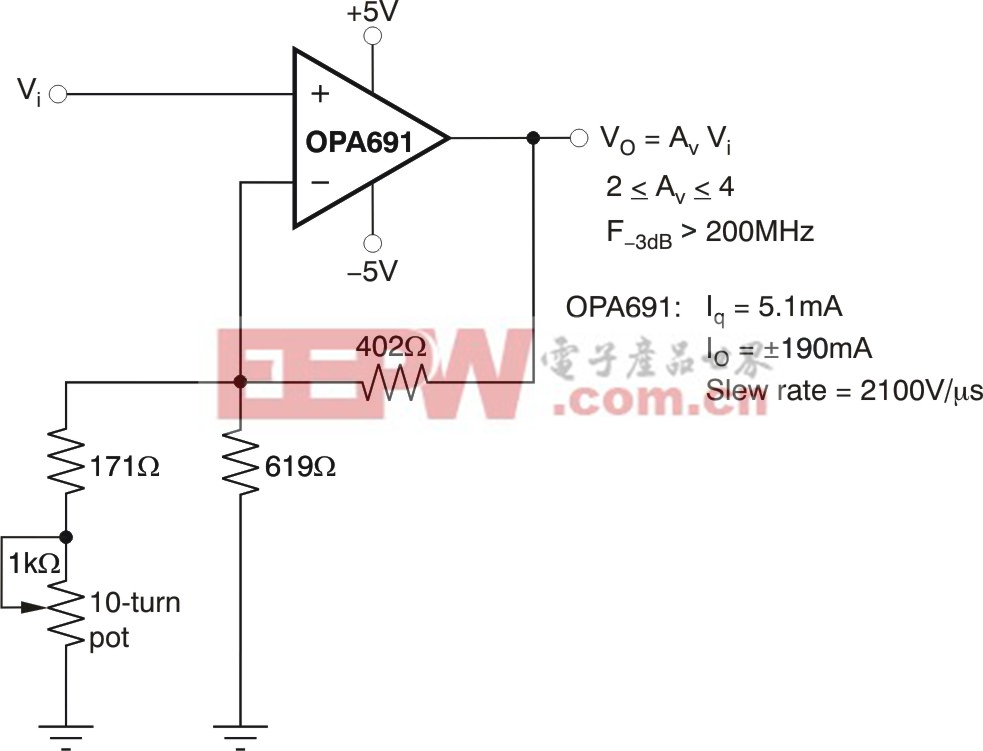
Where the gain needs to be adjusted, a CFB amplifier is preferred because it holds more constant bandwidth as that adjustment is made.Figure 7shows an example non-inverting design where the adjustment is configured to provide a fine-scale tune from a gain of +2 to +4 V/V using a high output current OPA691.
(Click to Enlarge Image)
Figure 7. Adjustable gain using the high output current OPA691.

加入微信
获取电子行业最新资讯
搜索微信公众号:EEPW
或用微信扫描左侧二维码