Freescalei.MX28家庭能量管理(HEM)平台设计方案
Freescale公司的家庭能量管理(HEM)平台采用i.MX283应用处理器,MC13224V ZigBee模块,9S08QE32 MCU和MC34726DC/DC降压转换器,用来开发家庭局部网络(HAN),包括基于i.MX283的控制板,可连接到智能电表,家庭自动化系统,宽带IP网络和用户接口等.本文介绍了i.MX28主要特性,框图,以及i.MX28/MC13224V家庭能量管理(HEM)平台主要特性,框图,详细电路图和设计文件.
The i.MX28 is a low-power, high-performanceapplications processor optimized for the generalembedded industrial and consumer markets. The core ofthe i.MX28 is Freescale’s fast, power-efficientimplementation of the ARM926EJ-S™ core, withspeeds of up to 454 MHz.
The device is suitable for a wide range of applications,including the following:
• Human-machine interface (HMI) panels:industrial, home
• Industrial drive, PLC, I/O control display, factoryrobotics display, graphical remote controls
• Handheld scanners and printers
• Patient-monitoring, portable medical devices
• Smart energy meters, energy gateways
• Media phones, media gateways
The integrated power management unit (PMU) on thei.MX28 is composed of a triple output DC-DC switchingconverter and multiple linear regulators. These providepower sequencing for the device and its I/O peripheralssuch as memories and SD cards, as well as provide battery charging capability for Li-Ion batteries.
The i.MX28 processor includes an additional 128-Kbyte on-chip SRAM to make the device ideal foreliminating external RAM in applications with small footprint RTOS.
The i.MX28 supports connections to various types of external memories, such as mobile DDR, DDR2 andLV-DDR2, SLC and MLC NAND Flash.
The i.MX28 can be connected to a variety of external devices such as high-speed USB2.0 OTG, CAN,10/100 Ethernet, and SD/SDIO/MMC.
i.MX28主要特性:
• ARM926EJ-S CPU running at 454 MHz:
— 16-Kbyte instruction cache and 32-Kbyte data cache
— ARM embedded trace macrocell (CoreSight™ ETM9™)
— Parallel JTAG interface
• 128 KBytes of integrated low-power on-chip SRAM
• 128 KBytes of integrated mask-programmable on-chip ROM
• 1280 bits of on-chip one-time-programmable (OCOTP) ROM
• 16-bit mobile DDR (mDDR) (1.8 V), DDR2 (1.8 V) and LV-DDR2 (1.5 V), up to 205 MHz DDRclock frequency with voltage overdrive
• Support for up to eight NAND Flash memory devices with up to 20-bit BCH ECC
• Four synchronous serial ports (SSP) for SDIO/MMC/MS/SPI: SSP0, SSP1, SSP2, and SSP3. SSP0and SSP1 can support three modes,1-bit, 4-bit, and 8-bit, whereas SSP2 and SSP3 can support only1-bit and 4-bit modes.
• 10/100-Mbps Ethernet MAC compatible with IEEE Std 802.3™:
— Single 10/100 Ethernet with GMII/RMII or Dual 10/100 Ethernet with RMII interface
— Supporting IEEE Std 1588™-compatible hardware timestamp
— Supporting 50-MHz/25-MHz clock output for external Ethernet PHY
• Two 2.0B protocol-compatible Controller Area Network (CAN) interfaces
• One USB2.0 OTG device/host controller and PHY
• One USB2.0 host controller and PHY
• LCD controller, up to 24-bit RGB (DOTCK) modes and 24-bit system-mode
• Pixel-processing pipeline (PXP) supports full path from color-space conversion, scaling,alpha-blending to rotation without intermediate memory access.
• SPDIF transmitter
• Dual serial audio interface (SAIF) to support full-duplex transmit and receive operations; eachSAIF supports three stereo pairs
• Five application Universal Asynchronous Receiver-Transmitters (UARTs), up to 3.25 Mbps withhardware flow control
• One debug UART operating at up to 115 Kb/s using programmed I/O
• Two I2C master/slave interfaces, up to 400 kbps
• Four 32-bit timers and a rotary decoder
• Eight Pulse Width Modulators (PWMs)
• Real-time clock (RTC)
• GPIO with interrupt capability
• Power Management Unit (PMU) supports a triple output DC-DC switching converter, multiplelinear regulators, battery charger, and detector.
• 16-channel Low-Resolution A/D Converter (LRADC). There are 16 physical channels but they canonly be mapped to 8 virtual channels at a time.
• Single channel High Speed A/D Converter (HSADC), up to 2 Msps data rate
• 4/5-wire touchscreen controller
• Up to 8X8 keypad matrix with button-detect circuit
• Security features:
— Read-only unique ID for Digital Rights Management (DRM) algorithms
— Secure boot using 128-bit AES hardware decryption
— SHA-1 and SHA256 hashing hardware
— High assurance boot (HAB4)
• Offered in 289-pin Ball Grid Array (BGA)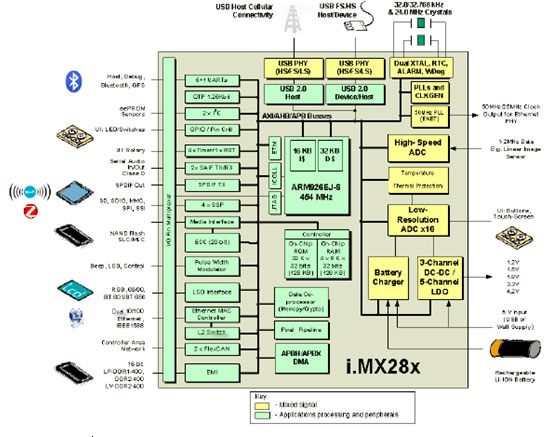
图1.i.MX28框图
i.MX28/MC13224V- 家庭能量管理(HEM)平台
Freescale’s Home Energy Manager (HEM) reference platform features an i.MX283 Applications Processor, MC13224V ZigBee® module, 9S08QE32 MCU and MC34726 DC/DC buck. The reference platform is aimed at jumpstarting customer developments around the HAN (Home Area Network).
It comprises of a control board based on the low-power, yet powerful i.MX283 running connectivity interfaces to the:
Smart meter
Home automation system
Broadband IP network
User interface
Micro-grid generation unitand includes software enablers (board support package and sample code)
In order to accomodate for a fast-pace changing connectivity landscape, the control board features extension connectors ready for :
Powerline modems
GPRS/3G data modem
U-SNAP connectivity peripherals
Mass storage cards
The complete reference design is available to designers at a cost of $650, thru the Adeneo Embedded web site, and includes a complete set of documentation, including a bill of materials, schematics, and reference manual. The demonstration software and the rich-OS BSP (Linux® and Windows® Embedded Compact 7) are available in source code format to registered users.
家庭能量管理(HEM)平台主要特性:
Low-power
Based on the latest low-power Freescale ARM9™ i.MX283 processor including integrated power management and supporting advanced voltage and frequency scaling techniques for optimized power consumption
Running Freescale’s low-power ZigBee radio
1.5W max at full operating speed
Low-cost
Unique integration on the i.MX283 eliminates external components, enables 4-layer PCB
Complete solution available
Source code
Hardware schematics
Gerbers
Bill of materials
Complimentary software available through 3rd party partners
Linux based frameworks
Windows Embedded Compact 7 based framework
Java based framework
Remote In-Home Display software
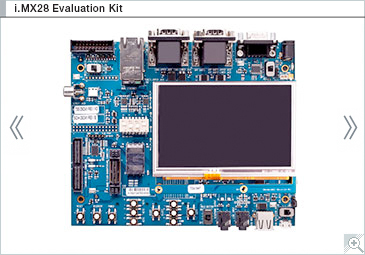
图2.家庭能量管理(HEM)平台i.MX28评估板外形图
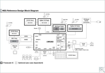
图3.家庭能量管理(HEM)平台框图
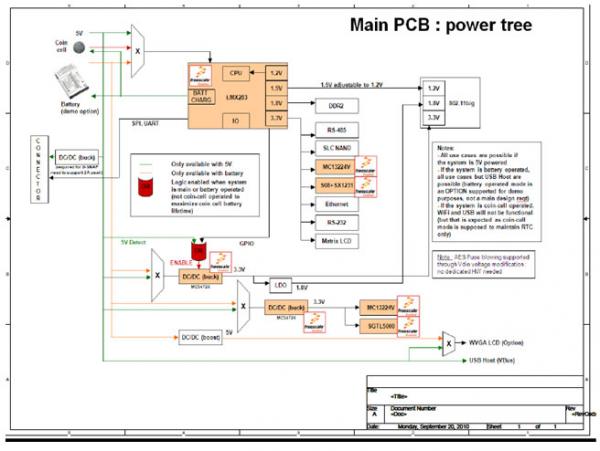
图4.家庭能量管理(HEM)平台主板电源树框图
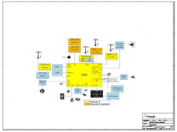
图5.家庭能量管理(HEM)平台电路图(1)
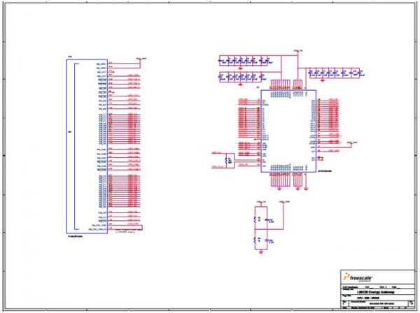
图6.家庭能量管理(HEM)平台电路图(2)
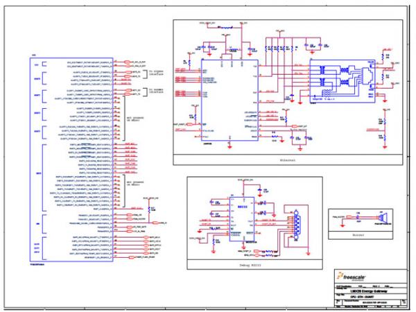
图7.家庭能量管理(HEM)平台电路图(3)
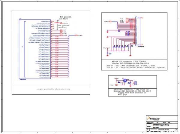
图8.家庭能量管理(HEM)平台电路图(4)
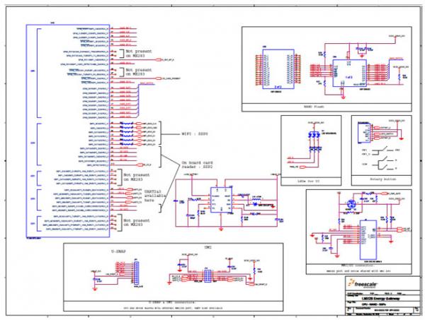
图9.家庭能量管理(HEM)平台电路图(5)
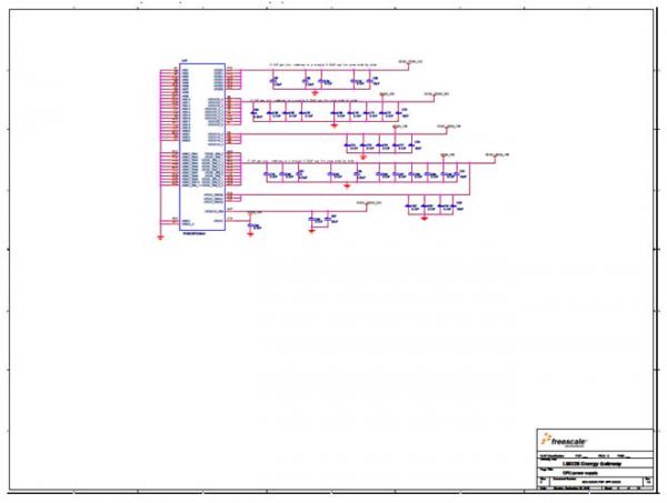
图10.家庭能量管理(HEM)平台电路图(6)

加入微信
获取电子行业最新资讯
搜索微信公众号:EEPW
或用微信扫描左侧二维码

