真空荧光显示器件参考设计为汽车应用-Vacuum Fl
作者:dolphin
时间:2011-07-20
Abstract: This article describes a vacuum fluorescent display (VFD) and some ideal applications for the technology. The reference design then shows how to use a MAX15005 power-supply controller in a flyback topology to obtain multiple output voltages for a vacuum fluorescent display.
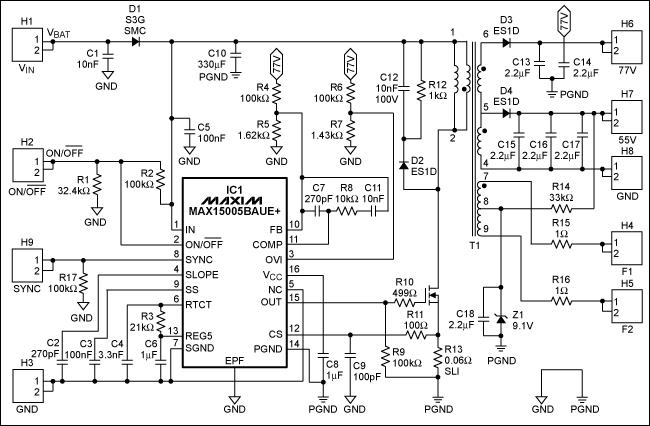
Figure 1. Schematic of the MAX15005B flyback converter for FSW = 22kHz.
The bill of materials (BOM) for this reference design is given in Table 1.
Table 1. Bill of Materials for VFD Reference Design
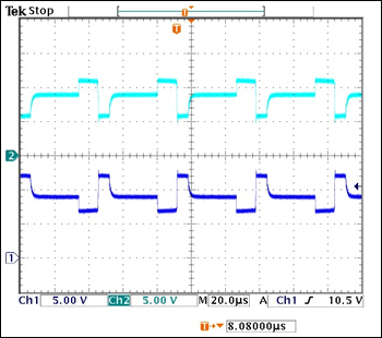
Test conditions: VIN = 14V; RANODE = 3.3kΩ; RGRID = 3.3kΩ; RFILAMENT = 8Ω.
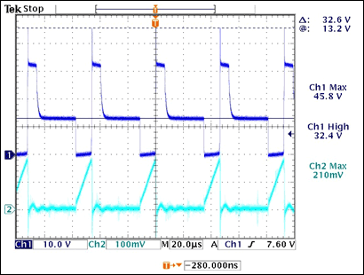
Ch1: MOSFET Q1 drain voltage (VDRAIN); Ch2: current-sense voltage across R13 (VISENSE).
Test conditions: VIN = 14V; RANODE = 3.3kΩ; RGRID = 3.3kΩ; RFILAMENT = 8Ω.
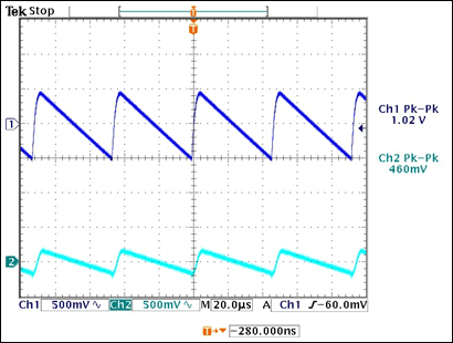
Ch1: anode output voltage ripple; Ch2: grid output voltage ripple.
Test conditions: VIN = 14V; RANODE = 3.3kΩ; RGRID = 3.3kΩ; RFILAMENT = 8Ω.
Ch1: filament positive node voltage (VF1); Ch2: filament negative node voltage (VF2).
Test conditions: VIN = 14V; RANODE = 3.3kΩ; RGRID = 3.3kΩ; RFILAMENT = 8Ω.
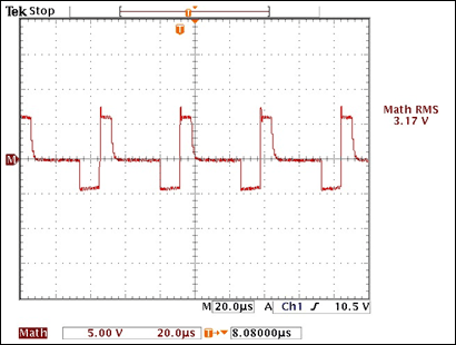
M: effective filament voltage (VF1 - VF2)
Introduction
This reference design shows a solution for obtaining the drive voltage required for a vacuum fluorescent display (VFD) power supply in automotive applications. The design includes the complete schematic, and presents the bill of materials (BOM), load/line regulation measurements, and test results.VFD Basics
The VFD is composed of three basic electrodes—the cathode filaments, anodes (phosphor), and grids—under a high-vacuum condition in a glass envelope. The cathode consists of fine tungsten wires, coated by alkaline earth metal oxides which emit electrons. The grids are a thin metal mesh, which controls and diffuses electrons emitted from the cathode. The anodes are conductive electrodes on which the phosphor is printed to indicate characters, icons, or symbols. Electrons emitted from the cathode are accelerated with positive potential applied to both grid and anode; upon collision with the anode the electrons excite the phosphor to emit light. The desired illuminated patterns can be achieved by controlling the positive or negative potentials on each grid and anode. The anode and grid require a DC-regulated voltage to avoid flickering of the display. For driving large VFDs, the cathode requires AC drive to prevent luminance slant, i.e., the difference in brightness from one side of the display to the other. A frequency range of 20kHz to 200kHz is recommended to avoid audible noise and flicker.Design Specifications and Setup
This reference design features the MAX15005 power-supply controller optimized for automotive and VFD applications. The application circuit is designed to meet the following specifications:- VIN: 9V to 16V continuous, 5.5V to 40V transient
- VANODE: 77VDC ±10% at 18mA (typ), 58mA (max)
- VGRID: 55VDC ±10% at 14mA (typ), 41mA (max)
- VFILAMENT: 3.1VAC ±10% at 350mA (typ), 385mA (max)
- Output ripple: 77V: 1VP-P; 55V: 0.5VP-P
- Line regulation, VIN = 9V to 16V:
VANODE = ±3%
VGRID = ±3%
VFILAMENT = ±5% - Load regulation: (see Line/Load Regulation Data section below)
- Switching frequency: 22kHz
- Temperature: -40°C to 125°C
Figure 1. Schematic of the MAX15005B flyback converter for FSW = 22kHz.
The bill of materials (BOM) for this reference design is given in Table 1.
Table 1. Bill of Materials for VFD Reference Design
| Designator | Value | Description | Part Number | Footprint | Manufacturer | Quantity |
| C1, C11, C12 | 10nF, 100V | Capacitor | C2012X7R2A103K | 0805 | TDK® | 3 |
| C2, C7 | 270pF, 100V | Capacitor | GRM188R72A271KA01D | 0805 | Murata® | 2 |
| C3, C5 | 100nF, 100V | Capacitor | C2012X7R2A104K | 0805 | TDK | 2 |
| C4 | 3.3nF, 25V | Capacitor | 08053A332FAT2A | 0805 | AVX® Corporation | 1 |
| C6, C8 | 1µF, 50V | Capacitor | C3216X7R1H105K | 1206 | TDK | 2 |
| C9 | 100pF, 100V | Capacitor | GRM2165C2A101JA01D | 0805 | Murata | 1 |
| C10 | 330µF, 35V | Capacitor | – | SMD | TDK | 1 |
| C13, C14, C15, C16, C17, C18 | 2.2µF, 100V | Capacitor | GRM32ER72A225KA35L | 1210 | Murata | 6 |
| D1 | 3A, 400V | Diode | S3G | SMC | Vishay® | 1 |
| D2, D3, D4 | 1A, 200V | Diode | ES1D | SMA | Vishay | 3 |
| Q1 | 11A, 55V | n-FET | BUK92150-55A | – | NXP® | 1 |
| R1 | 32.4kΩ | Resistor | SMD, 5%, 0.125W | 0805 | KOA | 1 |
| R2, R9, R17 | 100kΩ | Resistor | SMD, 5%, 0.125W | 0805 | KOA | 3 |
| R3 | 21kΩ | Resistor | SMD, 1%, 0.125W | 0805 | KOA | 1 |
| R4, R6 | 100kΩ | Resistor | SMD, 1%, 0.250W | 1206 | KOA | 2 |
| R5 | 1.62kΩ | Resistor | SMD, 1%, 0.125W | 0805 | KOA | 1 |
| R7 | 1.43kΩ | Resistor | SMD, 1%, 0.125W | 0805 | KOA | 1 |
| R8 | 10kΩ | Resistor | SMD, 5%, 0.125W | 0805 | KOA | 1 |
| R10 | 499Ω | Resistor | SMD, 1%, 0.125W | 0805 | KOA | 1 |
| R11 | 100Ω | Resistor | SMD, 5%, 0.125W | 0805 | KOA | 1 |
| R12 | 1kΩ | Resistor | SMD, 1%, 0.333W | 1210 | KOA | 1 |
| R13 | 0.06Ω | Resistor | SMD, 1%, SL1 | SL1 | KOA | 1 |
| R14 | 33kΩ | Resistor | SMD, 5%, 0.125W | 0805 | KOA | 1 |
| R15, R16 | 1.0Ω | Resistor | SMD, 1%, 0.250W | 1206 | KOA | 2 |
| T1 | 54µH | Transformer | DCT20EFD-UxxSOA5 | SMD | TDK | 1 |
| Z1 | 9.1V | Zener diode | 1SMB5924BT | SMB | Vishay | 1 |
| IC1 | MAX15005B | Boost controller | MAX15005BAUE+ | 16TSSOP | MAXIM® | 1 |
Waveform Measurements
The following test results were generated from the board built for evaluating the circuit.Test conditions: VIN = 14V; RANODE = 3.3kΩ; RGRID = 3.3kΩ; RFILAMENT = 8Ω.
Ch1: MOSFET Q1 drain voltage (VDRAIN); Ch2: current-sense voltage across R13 (VISENSE).
Test conditions: VIN = 14V; RANODE = 3.3kΩ; RGRID = 3.3kΩ; RFILAMENT = 8Ω.
Ch1: anode output voltage ripple; Ch2: grid output voltage ripple.
Test conditions: VIN = 14V; RANODE = 3.3kΩ; RGRID = 3.3kΩ; RFILAMENT = 8Ω.
Ch1: filament positive node voltage (VF1); Ch2: filament negative node voltage (VF2).
Test conditions: VIN = 14V; RANODE = 3.3kΩ; RGRID = 3.3kΩ; RFILAMENT = 8Ω.
M: effective filament voltage (VF1 - VF2)
Line/Load Regulation Data
The following line/load regulation data was taken from the test board over the input voltage range and load.| VIN | I77 (mA) | I55 (mA) | V77 (VDC) | V55 (VDC) | VF (VRMS) |
| 9.0 | 7.7 | 5.5 | 77.0 | 55.2 | 2.41 |
| 7.7 | 16.7 | 77.0 | 55.0 | 2.64 | |
| 7.7 | 44.0 | 77.0 | 54.8 | 3.03 | |
| 23.0 | 5.5 | 77.0 | 55.4 | 2.82 | |
| 23.0 | 16.7 | 77.0 | 55.2 | 2.97 | |
| 23.0 | 44.0 | 77.0 | 55.0 | 3.24 | |
| 61.6 | 5.5 | 77.0 | 55.8 | 3.35 | |
| 61.6 | 16.7 | 77.0 | 55.6 | 3.43 | |
| 61.6 | 44.0 | 77.0 | 55.4 | 3.62 | |
| 14.0 | 7.7 | 5.5 | 77.0 | 55.2 | 2.52 |
| 7.7 | 16.7 | 77.0 | 55.0 | 2.75 | |
| 7.7 | 44.0 | 77.0 | 54.8 | 3.14 | |
| 23.0 | 5.5 | 77.0 | 55.4 | 2.80 | |
| 23.0 | 16.7 | 77.0 | 55.2 | 3.08 | |
| 23.0 | 44.0 | 77.0 | 55.0 | 3.36 | |
| 61.6 | 5.5 | 77.0 | 55.8 | 3.50 | |
| 61.6 | 16.7 | 77.0 | 55.7 | 3.59 | |
| 61.6 | 44.0 | 77.0 | 55.4 | 3.79 | |
| 16.0 | 7.7 | 5.5 | 77.0 | 55.2 | 2.63 |
| 7.7 | 16.7 | 77.0 | 55.0 | 2.86 | |
| 7.7 | 44.0 | 77.0 | 54.8 | 3.25 | |
| 23.0 | 5.5 | 77.0 | 55.4 | 3.04 | |
| 23.0 | 16.7 | 77.0 | 55.2 | 3.20 | |
| 23.0 | 44.0 | 77.0 | 55.0 | 3.49 | |
| 61.6 | 5.5 | 77.0 | 54.8 | 3.25 | |
| 61.6 | 16.7 | 77.0 | 55.0 | 3.49 | |
| 61.6 | 44.0 | 77.0 | 55.4 | 3.92 |
Conclusion
This application note presents a power-supply reference design for driving a typical vacuum fluorescent display in an automotive application. The design was built to the specifications presented here. The design was then tested. The circuit schematic, BOM, and typical waveforms have been presented.AVX is a registered trademark of AVX Corporation.
Maxim is a registered trademark of Maxim Integrated Products, Inc.
Murata is a registered trademark of Murata Manufacturing Co., Ltd.
NXP is a registered trademark of NXP Semiconductors.
TDK is a registered trademark of TDK Corporation.
Vishay is a registered trademark of Vishay Intertechnology, Inc.

加入微信
获取电子行业最新资讯
搜索微信公众号:EEPW
或用微信扫描左侧二维码